 |
Z80-PC - Page 1 |
|
Z80-PC - Page 1 |
This is a fun spare time project to recreate the experience of using a simple computer as was typical in the early 1980s. There are lots of such projects done with various objectives in mind, such as recreating a specific machine to be able to run legacy software; or for the purpose of nostalgia. I think, however, that one main reason for such a project is the fact that as systems become more complex, there is less sense of full control over the system. A modern machine is running a whole bunch of code and processes of which even a master user has little control or even perception. Therefore, creating a simple machine which provides full control over most if not all of its parts, has an appeal to people with an engineering aptitude. The main emphasis in this project to get something up and running, with as little complexity as possible. As the mantra goes “Keep It Simple, Stupid”
The most basic system possible is composed of a CPU with some clock source, and some memory. The CPU of choice here is the Zylog Z80, due to its availability, simplicity, and abundance of reference material online. The memory to be used is Static RAM (or SRAM), since Dynamic RAM is more complicated to work with. Later on we’ll be adding IO (Input Output) devices as well.
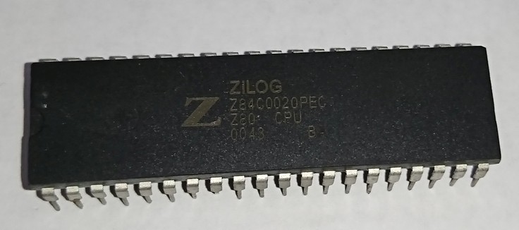
Going back to the KISS mantra, most components used in this project are of the through-hole type, meaning that using either a prototype board, or a printed circuit board (PCB), the component’s “legs” go through the board’s holes and soldered in place. In some cases, a mount is soldered to the board, and the component is inserted into the mount. The Z80 chip used here has a DIP (Dual Inline Package) with 40 legs, and therefore DIP-40. The indentation (semi-circle in this case) in one side indicates which side has pin #1. In the image above, the bottom left pin is #1, and the bottom row goes to the right until #20. Then the top row continues (from the right) for pins #21-#40
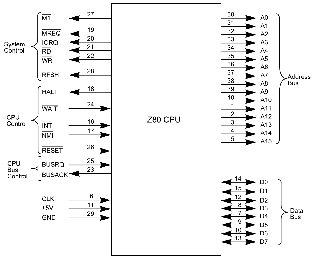
The schematic above shows what each of the pins do, also grouping them according to function. Since the manual provides excellent description of the pins function, we will not get into that.
As indicated above, the memory to be used in of Static RAM type. More specifically, we’ll be using a DS1245Y-70, which is a 128KB chip with a non-volatile feature. This means that when the power goes out, it keeps its contents. So, there is no need to have a separate ROM and RAM. On the other hand, a program that corrupts the system memory will require rewriting the system before the machine can be used again. Perhaps at a later iteration, the memory will be replaced by the traditional ROM/RAM combo. The 70 in the chip’s designation indicates the memory access latency of 70ns. For any CPU that has a clock speed of less than 10MHz, as this will, this means the CPU doesn’t have to wait multiple cycles for the memory. Makes things simple. Also, even though this memory chip has 128KB, we’ll only be using the bottom 64KB.