|
Z80-PC - Page 3 |
|
Z80-PC - Page 3 |
The block diagram in the previous post is really low on details, so it’s time to get into those. There are a lot of options to edit and design the schematics and printed circuit boards (PCB), and the one I use is an online tools on http://easyeda.com It allows you to place the components, connect them, and then create a PCB from your design, and even send it to be manufactured. So, the schematic for the CPU and memory as described previously is given in the following schematic:
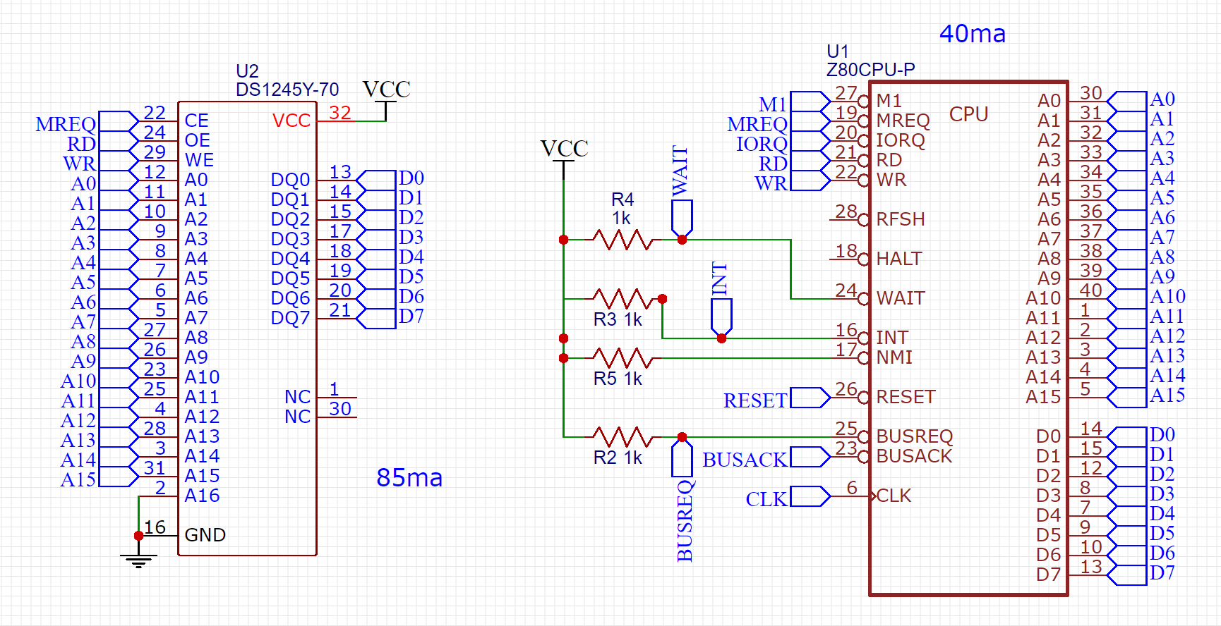
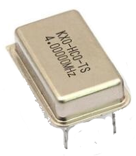
Although it is possible to connect everything with wires, using nets (those blue endpoints) is much more readable and usable. Basically, when two nets have the same name, they are assumed to be connected. So, this schematic shows that the address and data bus of the CPU connect directly to the memory, except for the RAM’s A16 pin, which allows usage of the entire 128KB range. Currently it’s unused. As mentioned previously, the MREQ signal enables the RAM, the RD signal allows the RAM to output data to the bus, and the WR signal indicates to the RAM that the memory should be written. On the CPU side, unused outputs can be left unconnected, like the RFSH (which is used for DRAM) and HALT (which is used to indicate shut down). Unused inputs much be connected (according to each pin’s spec) to either VCC or ground (Usually VCC), preferably using a pull-up resistor. In our case there are 4 such pins: INT, NMI (used for interrupts), RESET (as the name indicates), and BUSREQ (which is used by devices to ask the CPU permission to use the bus for their own needs). Note that some of these also have nets connected, which will be used later on. The CLK input needs to get the CPU clock, which will be generated by an oscillator integrated circuit. This component takes VCC and ground, and outputs the CLK signal on the appropriate pin.
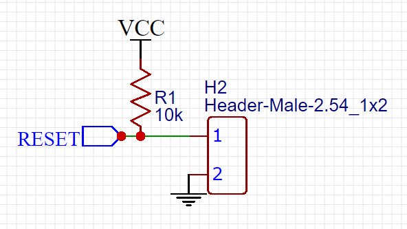
The RESET pin should be connected to a circuit that usually connects the pin to VCC, except when actually doing a reset, then the pin should be connected to ground. The following circuit accomplished that, by connecting the pin to VCC using a pull-up resistor. The header is used to connect the pin to ground through a button. The reason a header is used, is to allow the button to be located off-board, like on the case front.
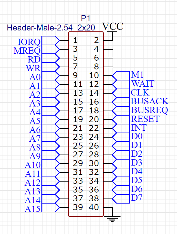
Though it is possible to place all the component for this computer on a single board, I have decided to split it into multiple boards, mainly to allow easier debugging. First, if one board is malfunctioning, the rest may still work without it. Also, if one board has a mistake, it’s possible to fix only that and there’s no need to re-manufacture the entire computer board. In order to connect the boards, large headers are placed on the main board, which act as expansion card slots. Each such header has 2×20 pins, allowing connections of all CPU pins. On a small 10x10cm main board, there is room for 3 such slots, though I would probably only use 2.