 |
Z80-PC - Page 4 |
|
Z80-PC - Page 4 |
A computer that runs code but has no way to get users input, or produce some noticeable output is not very useful. Therefore, the computer must have some means to receive and send information to the outside world.
Originally, I had the intention to only include the simplest form of I/O, which is some form of serial communication, which would allow to access the computer from another machine, using some terminal software. I had some salvaged chips from old machines, and found among them a universal asynchronous receiver transmitter (UART) chip 8250. This was used in early 80s machines. Going over its datasheet and some online schematics, I came to the conclusion it would be easier to use some micro-controller for this purpose, and will also allow to perform more than just serial communication. Since I'm not a purist trying to recreate a specific machine, or limit myself to chips that were available up to some point, I decided to use an AVR micro-controller (MCU) as a UART.
The way output works on the z80 is that when an output instruction is processed, the CPU places the IO address on the address bus, places the data to be written on the data bus, and uses the IORQ pin to indicate that an IO operation is being executed. Any IO device that corresponds to the given address, should take the data and do what it needs with it. Unlike writing to memory, the response time of a micro-controller can be somewhat longer, which causes a problem, since the address and data are only on the bus for a limited time while the instruction is executed.
One possible solution to this problem is to use the WAIT pin to stop the CPU while the data is processed. I decided not to use that option, but instead, use a latch to retain the information needed until it is consumed by the MCU. A latch is like a tiny memory chip, and in this case, a single byte. One example of a latch chip is the 74HCT573.
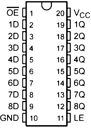
The D0-D7 pins simply connect to the data bus, but until the LE pin is high, the chip ignores the data bus. When the LE goes high, the chip will retain the contents of the data bus until the next time LE goes high. What ever is stored in the chip's memory, is not written to the Q0-Q7 outputs until the OE (output enable) pin goes low. So, how do we connect this chip to the CPU? We need to look at the IO timing chart from the manual.
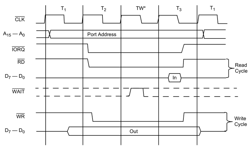
As can be seen in the write cycle, the condition for getting the data from the bus is composed of the following 3 parts:
The combination of these conditions can be accomplished using logical gates, but since we need quite a few of these, all gates will be replaced by a single SPLD chip (ATF22V10).
This chip allows programming a boolean expression that combines multiple input pins and output the resulting value. Programming is done using software like WinCUPL and writing to the chip in a similar fashion to writing to a ROM chip.
For the purpose of the LE signal, we can define it as:
LE = !IORQ & !WR & !A0 & !A1 & !A2
This means that the address is checked to be 0, in a 0-7 range, ignoring higher address bits.
The LE signal that the latch uses to store the data can also be connected to the MCU interrupt pin so that it knows a new byte is being written, and it can then apply (through an IO pin) the OE signal and read (using 8 pins) the data.
Input is a little more complex. Placing the data on the data bus is pretty much the same as was done with the output, but letting the CPU know that input is available and having it process the input requires the usage of interrupts. The z80 has several interrupt modes, which are documented in the manual. For simplicity, in this computer only mode 0 is going to be used. In this mode, when an interrupt occurs, the CPU requests from the device an instruction to be run. The request takes the form of a combination of M1 and IORQ signals. Luckily, there is a single byte instruction called RST which allows the calling of a service routine to process the input.
So, for the input, 2 latches are used. One to hold the instruction to call the service routine, and one to hold the incoming data byte. The MCU fills both of them prior to signalling an interrupt to the CPU. Once the second latch is filled, the LE signal of that latch can also be connected (inverted / active low) to the CPU interrupt pin.
If multiple inputs are used, the RST instruction parameter can be used to differentiate between the inputs.